
Unlocking Efficiency: GaN Technology for Lower Driving Costs and Higher Power
Gallium nitride (GaN) technology is making significant strides in the high-voltage, wide-bandgap power field, challenging the dominance of silicon carbide. The shift towards GaN is primarily driven by lower costs and processes that are more compatible with bulk silicon, opening up new opportunities for efficiency, power density, and cost savings in power electronics.
Efficiency, power density, and cost are the key considerations in power electronics, and GaN has shown promise in meeting all three criteria. However, to consistently deliver on these fronts, the semiconductor ecosystem must establish best practices for testing, inspection, and metrology to determine the optimal applications and conditions for GaN technology.
Power integrated circuits (ICs) play a crucial role in voltage conversion from one power source to another, with GaN already widely used in smartphone and laptop adapters. The market opportunities for GaN technology are expanding, particularly in data centers and automotive applications. The rapid growth of data centers driven by AI and edge computing demands efficient power solutions, while the automotive industry sees potential in using GaN power ICs for inverter modules, onboard battery chargers (OBCs), and various DC-DC conversions within vehicles.
To tap into new markets, GaN device manufacturers need to accelerate the development of new processes and products. As GaN for power transistors is still evolving, comprehensive measurement data is essential to validate the manufacturing process and ensure the reliability of the technology and resulting products.
While silicon carbide remains the material of choice for high-voltage applications due to its superior performance and efficiency compared to silicon, GaN offers similar advantages and can operate at even higher switching speeds. GaN wafer production is cost-effective as it can be created on a silicon substrate using conventional silicon processing equipment, making it accessible to fabs and foundries with expertise in GaN technology.
The cost comparison between GaN and SiC varies, with GaN demonstrating a cost advantage at lower voltages. GaN’s potential for cost-effectiveness has reignited interest in the technology, particularly as it continues to expand into new application spaces.
GaN-based products offer enhanced performance compared to traditional silicon technologies, enabling new possibilities in power electronics. The ability of GaN to operate at high switching speeds unlocks innovative applications that were previously unattainable with silicon. As production volumes of GaN devices increase, there is a need to address economic challenges while harnessing the dynamic capabilities of GaN technology.
The future of GaN technology lies in expanding into higher voltage ranges, which necessitates the development of new process recipes, power IC designs, and rigorous product validation and qualification. Understanding the material properties and manufacturing implications of GaN high-electron-mobility transistors (HEMTs) is crucial for advancing GaN technology in higher operating ranges.
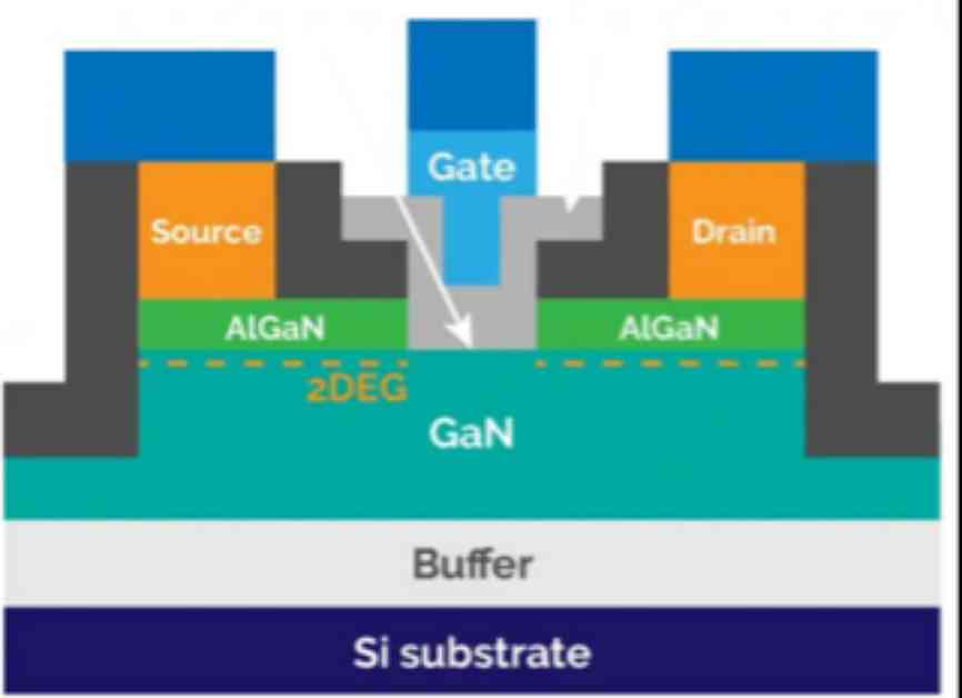
The unique structure and physics of wide-bandgap devices like GaN HEMTs require a deep understanding of material properties and precise control over the manufacturing process. GaN devices rely on a two-dimensional electron gas (2DEG) to conduct current at high speeds, necessitating meticulous monitoring and control of epitaxial processes to ensure optimal film properties.
Process recipes for GaN HEMT devices at higher operating ranges demand comprehensive measurements during wafer manufacturing and device testing for qualification and production. Inspection, metrology, and electrical tests play a pivotal role in identifying process anomalies and defects that impact device performance.
Reliability and lifetime validation of GaN power devices require a thorough understanding of device failure mechanisms and accelerated testing methods to predict device lifetimes accurately. Qualification procedures involve life-stressing testing and electrical assessments to assess shifts in transistor characteristics and ensure long-term reliability.
To address the unique challenges posed by GaN devices, specialized testing techniques are essential to screen for both static and dynamic defects that impact device performance and reliability. The stringent testing requirements for GaN devices necessitate innovative approaches to accelerate testing processes and reduce overall testing costs for manufacturers.
Tools for process control, yield management, and failure analysis are critical for optimizing GaN device performance and ensuring product quality. Non-destructive inspection methods, such as optical and X-ray techniques, provide valuable insights into film characteristics and defect identification for process improvement.
In conclusion, GaN technology holds immense potential for revolutionizing power electronics with its efficiency, power density, and cost advantages. By leveraging advanced metrology, inspection, and testing solutions, engineers can unlock the full capabilities of GaN technology and drive innovation in power applications across various industries.
References:
M. Buffolo et al., “Review and Outlook on GaN and SiC Power Devices: Industrial State-of-the-Art, Applications, and Perspectives,” in IEEE Transactions on Electron Devices, March 2024, open access
High electron mobility transistor (HEMT)
Guideline to specify a transient off-state withstand voltage robustness indicated in datasheets for lateral GaN power conversion devices, JEP186, version 1.0, December 2021


